AINA (Part 0): Why are we still sizing analog circuits by hand?
This blog series is a collaborative one (pun intended) between me and my LLMs. Rest assured, everything is human verified and I believe where LLM does give better explanation with brevity, have humility to accept it. Also, since this is also a way for me to learn, I have tried to keep it simple enough for a beginner to understand, but also cover enough depth to be interesting to an expert.
AI has advanced to a great extent presently. We have seen the recent capabilities in the agentic space, where a swarm of OpenAI agents formed their own civilizations to escape the sandbox and hack nodes on HuggingFace.
With such speed, it is only a matter of time that the next focus turns to applying these systems. Think of it like a growing tree: the trunk is continuously growing at a blazing speed (the main AI systems), and it has grown enough for new branches to blossom.
Recursively improving agents are a perceived threat and a far stronger force speeding towards improving itself. When agents are working hard enough to improve themselves, let me have the courtesy to give them a better country to live in. No, I won’t design the chips, but I propose to make the electronics industry speed up in terms of throughput and latency.
Digital Scaled, But Why Not Analog?
Both Digital and Analog are built from the same imperfect analog devices: transistors.
Digital engineering is powerful and easily scalable because it arranges those devices so that most of the transistor-level imperfections are absorbed by thresholds, noise margins, regeneration, and abstraction. It has very high error endurance due to the discrete nature of its input and output, whereas analog deals with the continuous space and is prone to error.
The Present Workflow
They say analog design is an art and the engineers, Michelangelo. I don't intend to replace these great artists, but provide them with better colors and brushes so that they can make more and better art.
An analog team primarily consists of two core engineering roles: the Analog Circuit Design Engineer and the Analog Layout Engineer.
The problem with this division is the high-friction feedback loop between them. The design engineer sizes the transistors in an ideal schematic environment, but once handed off to the layout engineer to draw physical masks, post-layout parasitic extraction (PEX) destroys the ideal performance. Unwanted interconnect capacitances, resistances, and layout-dependent stresses cause gain to collapse and phase margins to degrade. This forces an agonizing, high-latency "ping-pong" iteration: resize, redo layout, re-extract, and repeat—stretching what should be hours into weeks of manual adjustment.
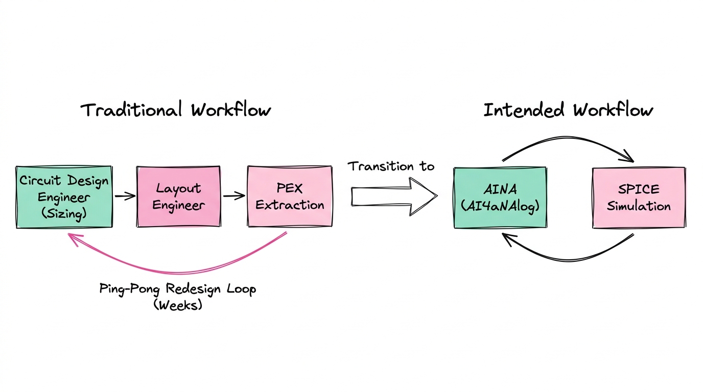
Goal
To make an agent who can design an analog circuit from scratch, and can work on it until it meets the desired specifications.
Self-Reflective Agent (LLM) + RLFT Capable Agent
LLM becomes the policy to optimize. We want agents that know numerical optimization and device physics as well at the same time.
Even human analog engineers rarely invent entirely new circuit structures from scratch. Instead, they choose a standard foundation (like a Differential Amplifier or a Miller OTA) and spend weeks doing the heavy mathematical work of sizing the components to match the target process node.
This is the motivation behind my agent: aina (AINA: AI4aNAlog).
Initially, I will focus on agent architecture and the choices along with the conclusions.